High-Reliability Multilayer PCB
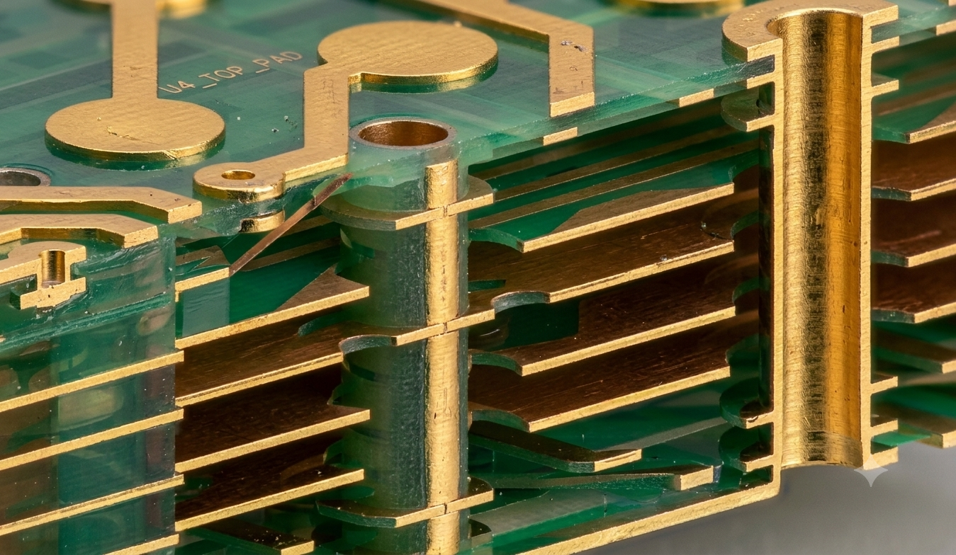
20 Layer · 1.6 mm · ENIG · Controlled Impedance · IPC Class 3
From PCB fabrication to component sourcing, SMT assembly, inspection, and global delivery — one accountable manufacturing partner in South Korea.
Our Engineering Commitment
Send us what you have. Our engineers will help complete the manufacturing data package.
Recommended files
※ Required: Please click the process(es) you need (multi-select)
Design in. PCBA out. Made in Korea. — PCB fabrication, component sourcing, SMT assembly and inspection managed through one accountable partner.
Predictable Workflow
Select a step to see exactly what happens and what you receive.
Send Gerber/ODB++, BOM, and Pick & Place data — or just a schematic. Files are encrypted in transit and handled confidentially, shared only with the assigned engineers.
SMT / PCBA
High-precision SMT for prototype, NPI and production.
Component Sourcing
Choose the sourcing model that fits your program — we manage the rest.
Complete component sourcing + PCB fabrication + assembly under one purchase order.
You supply all components; we handle kitting verification, fabrication, and assembly.
Customer-supplied critical parts combined with team-sourced commodity components.
No component substitution without customer approval.
PCB Fabrication
From quick-turn prototypes to high-reliability multilayers.
| PCB Type | Standard Specs | Advanced / Special Specs | Key Features |
|---|---|---|---|
| Heavy Oz | 2–8L | 10–18L | 3–10oz Copper Power Supply Board & Bus Bar |
| Metal Base | 1–2L (Al/Cu base) | 4–12L | Metal Plate High Heat Dissipation (Heat-sink) |
| BVH (Blind/Buried Via) | 4–12L | 14–24L | Blind Via Hole & Buried Via Hole |
| HDI | 6–8L | 10–16L | High-Technology Multilayer PCB |
| Flex-Rigid | 4–8L | 10–22L | High-Layer Flex-Rigid / HDI Flex-Rigid |
| High-Count Multilayer | 4–20L | 22–42L | High-Layer MLB & Probe Cards |
| Hybrid | ~8L | 10–24L | Special Materials (Rogers, Taconic, Nelco, Isola, PI) |
| Parameter | StandardNormally available | AdvancedAvailable by engineering review | MaximumProject-specific / factory confirmation |
|---|---|---|---|
| Layer Count | 2–20L | 22–32L | 34–42L |
| Board Thickness | 0.4–3.2 mm (16–126 mils) | 4.8 mm (190 mils) | Max 6.0 mm (240 mils) |
| Min Line Width / Space | 0.1 mm (4 mils) | 0.075 mm (3 mils) | 0.05 mm (2 mils) |
| Min Mechanical Hole Size | 0.25 mm (10 mils) | 0.15–0.2 mm (6–8 mils) | 0.1 mm (4 mils) |
| Min Laser Hole Size | 0.10 mm (4 mils) | 0.08–0.09 mm (3.15–3.54 mils) | 0.08–0.09 mm (3.15–3.54 mils) |
| Max Board Size | 507×607 mm (20×24″) | 600×800 mm (24×31″) | 600×800 mm (24×31″) |
| Impedance Control | ±10% | ±7% | ±7% |
Values are typical reference capabilities. Final confirmation is provided after engineering review and DFM analysis.
Quality
Know exactly what we check — and exactly what you receive.
Detailed DFM feedback is provided after receiving sufficient manufacturing data.
Lead Times & Logistics
DHL Express, FedEx, UPS, or your own freight forwarder — with DAP and DDP Incoterms options.
Manufactured in South Korea. Delivered worldwide.
Supply Chain Diversification
A stable, allied-nation manufacturing base with mature electronics infrastructure, engineering depth, and predictable export logistics.
Manufactured in South Korea through a qualified Korean manufacturing network under our engineering supervision and quality control — with full process traceability from fabrication to final inspection.
A trusted allied-nation alternative for defense and advanced tech programs, with IP strictly protected under Korean law.
English-fluent senior engineers answer within hours — no translation layers between your design intent and the production floor.
Technical Excellence
Specialized in Defense, Aerospace, and Industrial Grade. Expertise in Rigid-Flex PCBs and Multi-Layer builds from 2 to 42 layers.
Powered by state-of-the-art machinery and automated lines—including pulse plating and ultra-fine pattern tech—ensuring flawless precision for high-density builds.
Equipped for components down to 0201 (01005 available upon engineering review) and high-density mounting at up to 1.4 million placement points per day.
We don't just print your files — we review them and return a defect prevention proposal. DFM Review: 1–3 Business Days.
Quality & Security
A qualified Korean manufacturing network across Seoul, Incheon, and Ansan — orchestrated as a single production layer.

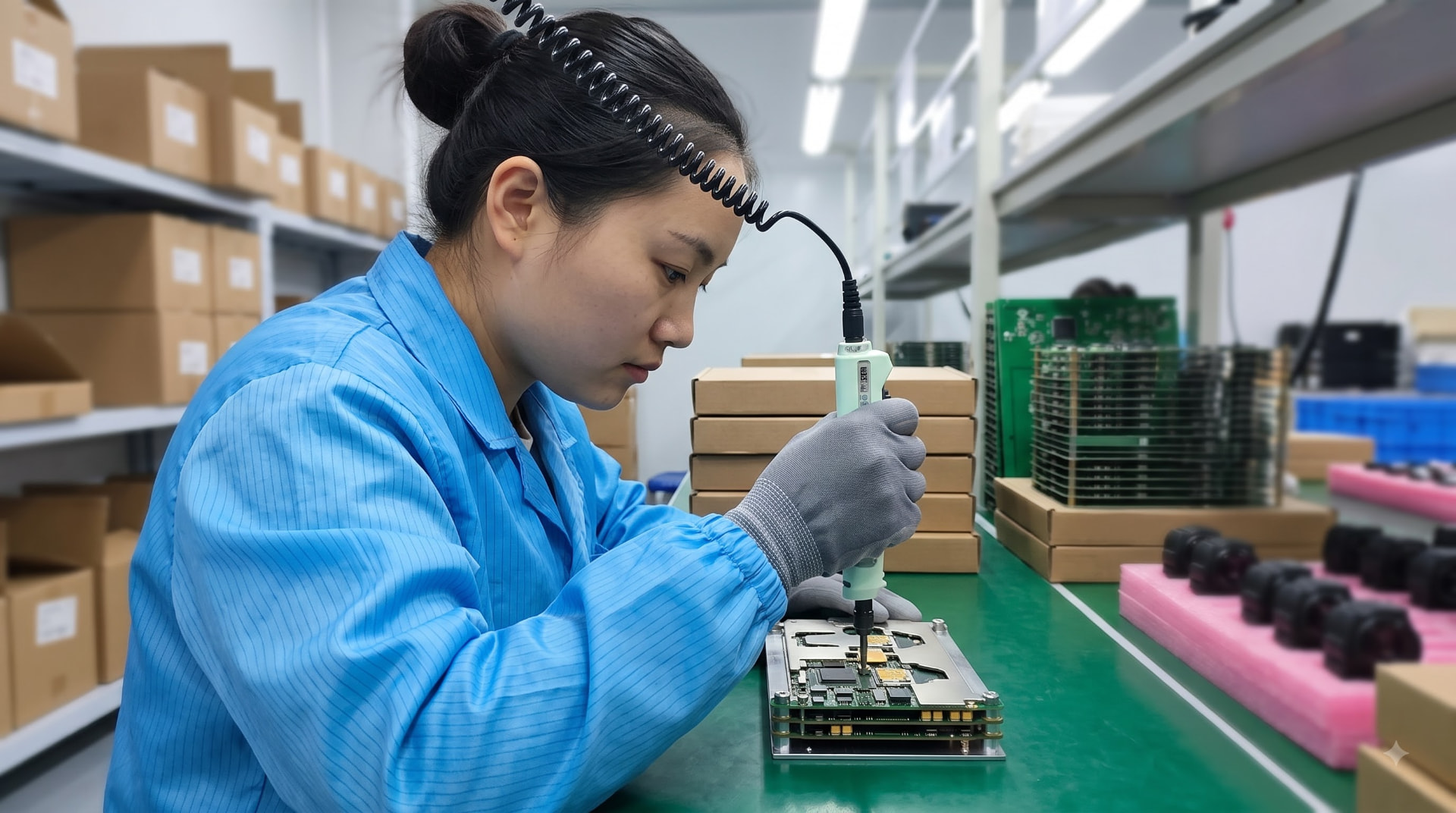
Manual PCB assembly with ESD protection and IPC Class 3 workmanship.

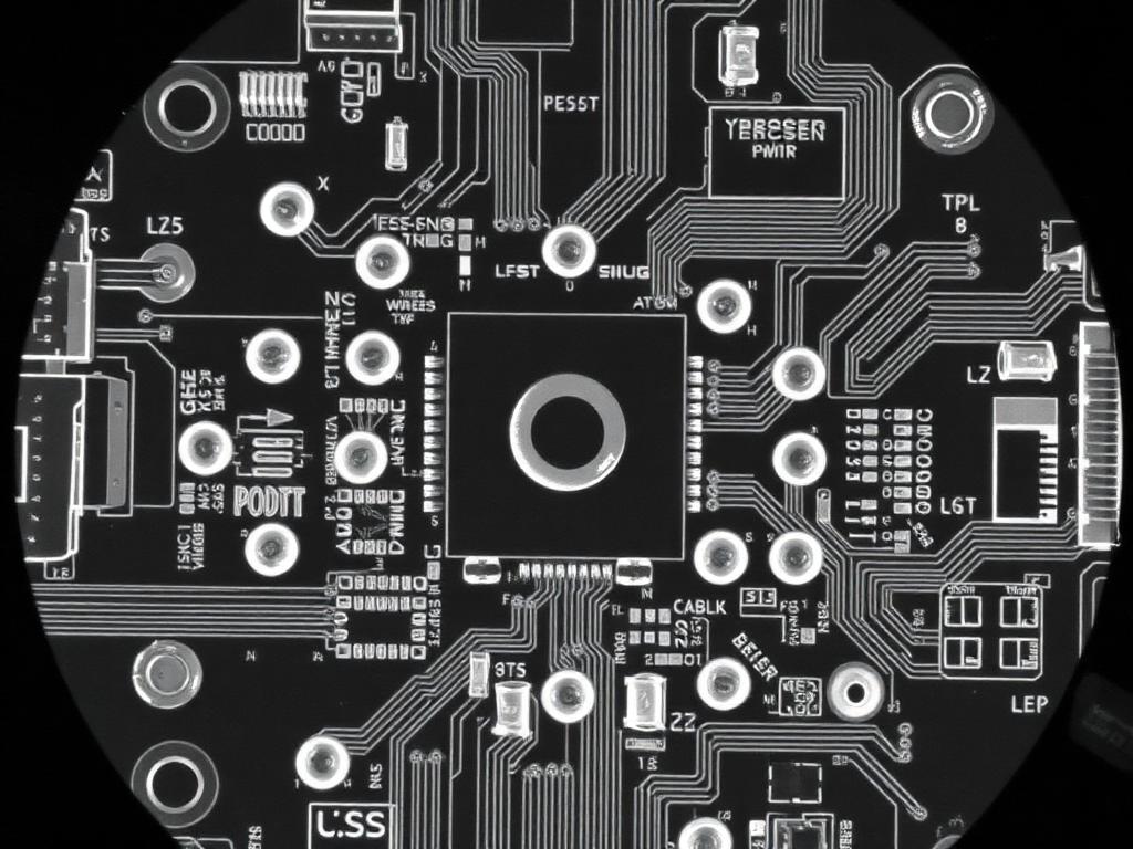
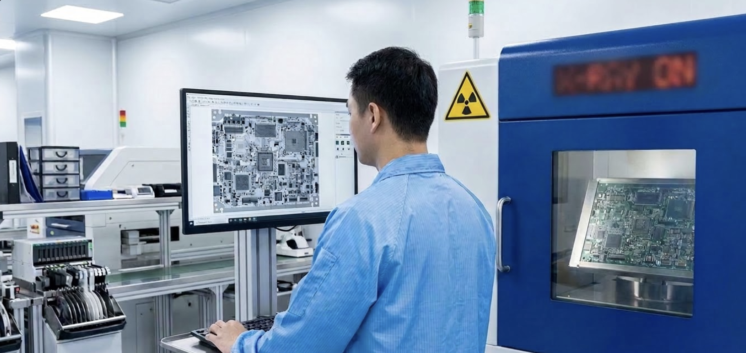
3D X-Ray and CT inspection for BGA, QFN and hidden solder joints — void ratio, bridging, and alignment verification.

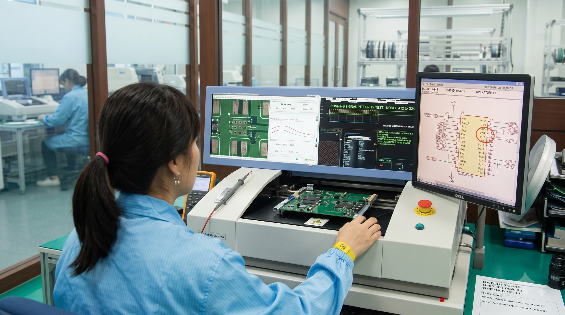
Automated optical inspection for component presence, polarity, offset, and solder fillet quality against IPC acceptance criteria.

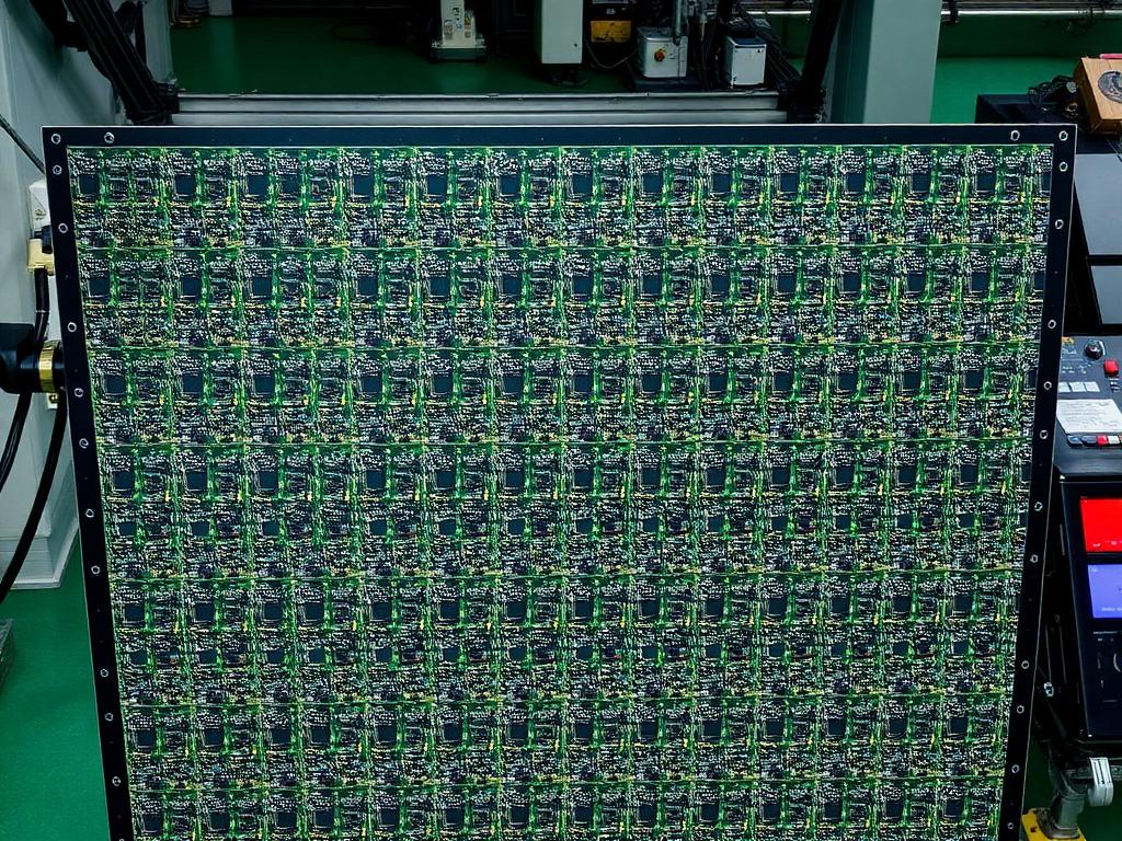
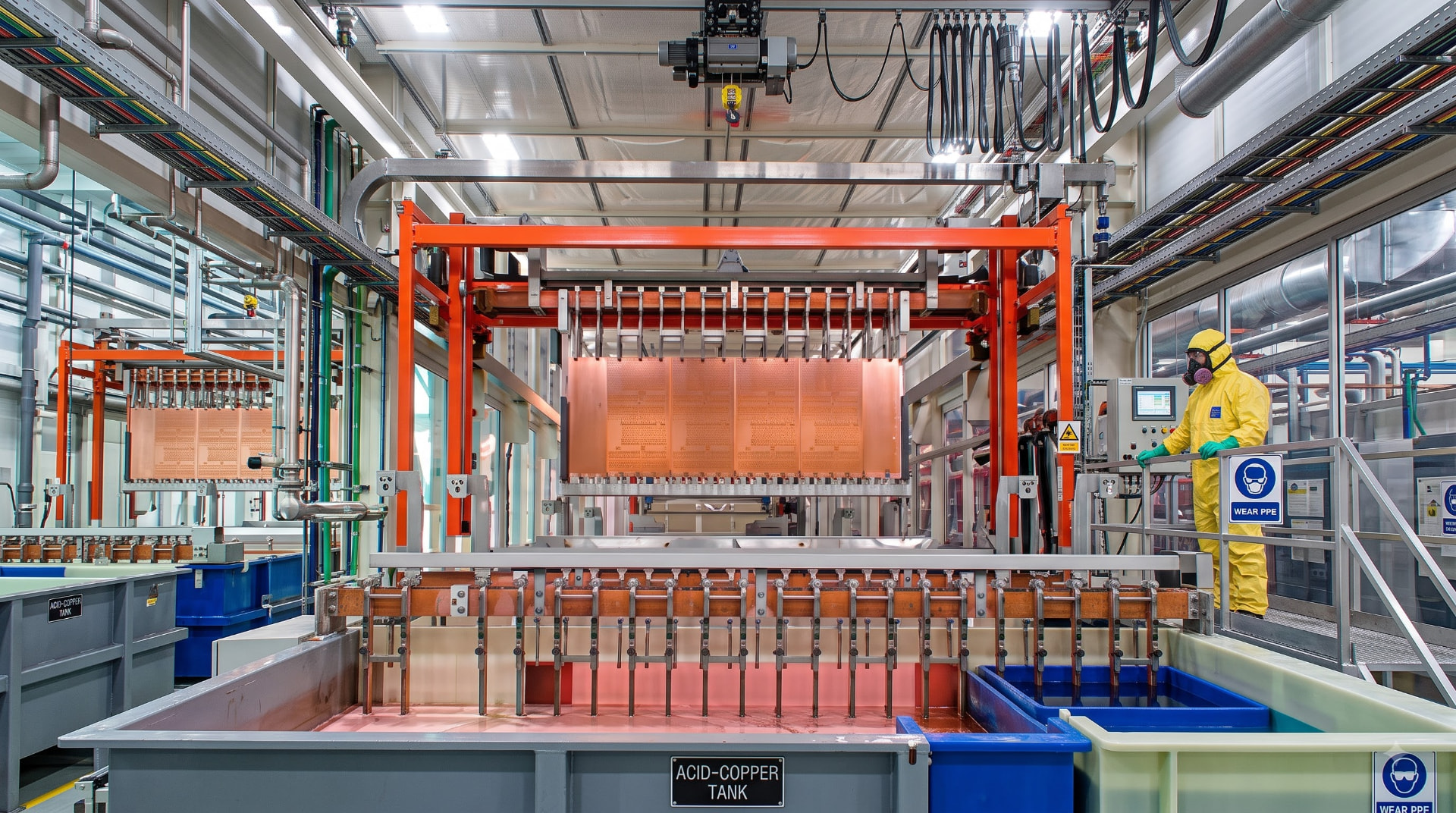
Automated acid-copper plating line for uniform deposition across high-density panels, maintaining consistent copper thickness ±5%.
Quality & Compliance
Certifications and standards applied across our qualified Korean manufacturing network.
All production within the NexTurnPCB network is strictly executed in compliance with these international quality standards and IPC workmanship guidelines.
Data Scope
Send what you have. We handle the rest of the data package.
What you send us
What we deliver back
Target Turnaround
Case Studies
Anonymized examples of typical builds handled by our Korean manufacturing network.
20 Layer · 1.6 mm · ENIG · Controlled Impedance · IPC Class 3
0.4 mm pitch BGA · 1,800 placements · SPI + AOI + 3D X-Ray
10 pcs prototype → 2,000 pcs/month · Frozen BOM · FAI documented
Representative process visuals


Illustrative process visuals — not customer-specific product photography.
FAQ
Find quick answers to common questions about our Korean PCB manufacturing, DFM process, and global services.
Send your files and get engineering feedback with a quote — DFM Review: 1–3 Business Days.
Detailed DFM feedback is provided after receiving sufficient manufacturing data.